Blinky PCB Design
During my second year of university, I participated in a club where I acquired foundational knowledge in PCB design. The Blinky PCB project consolidates all the skills in one project as shown below.
PCB Design
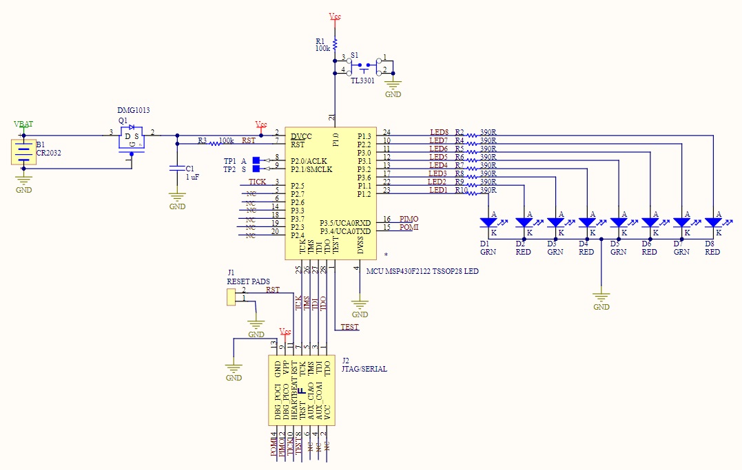 Schematic
Creating a schematic diagram of the circuit to outline what components exist, andhow they interact with eachother
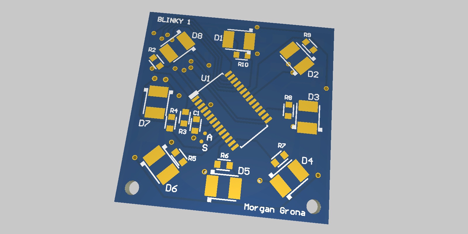
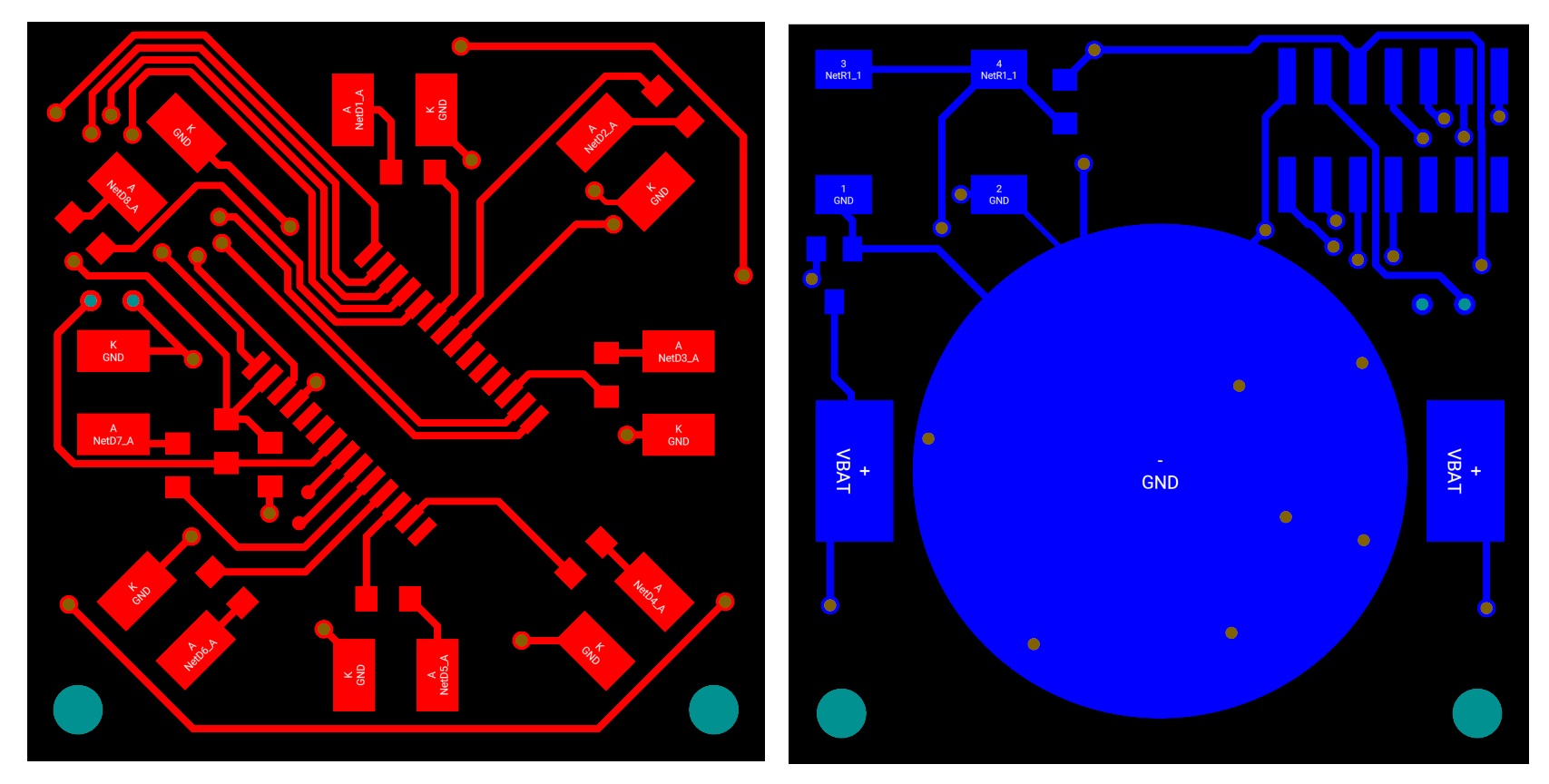 Component Routing
Routing all the parts together is like solving a puzzle. Following design rules and general best practices allows for effective routing.
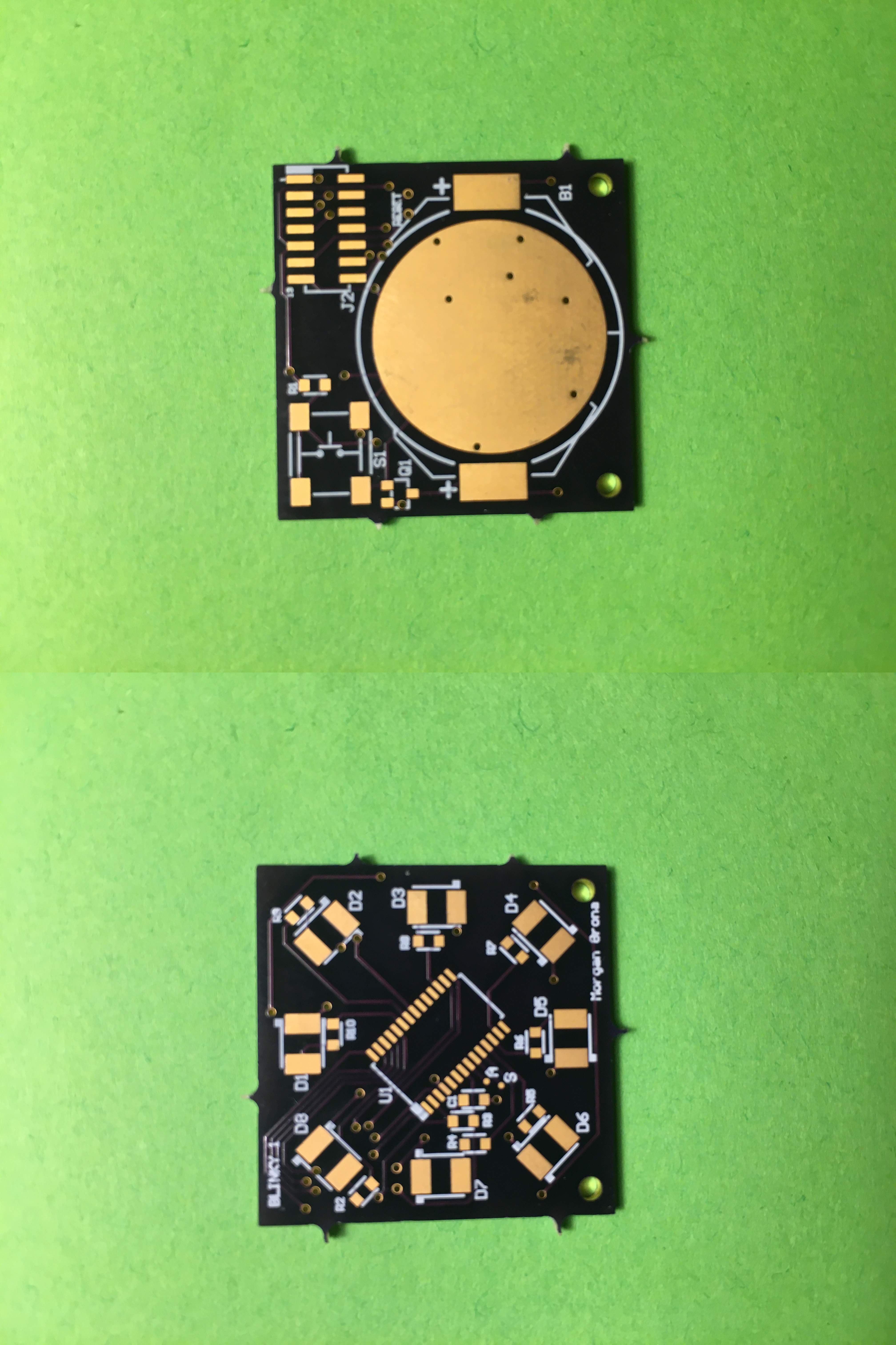 Blank Fabricated PCB
Unveiling a personally designed PCB brings immense joy after weeks of anticipation for fabrication and shipping.
Finished
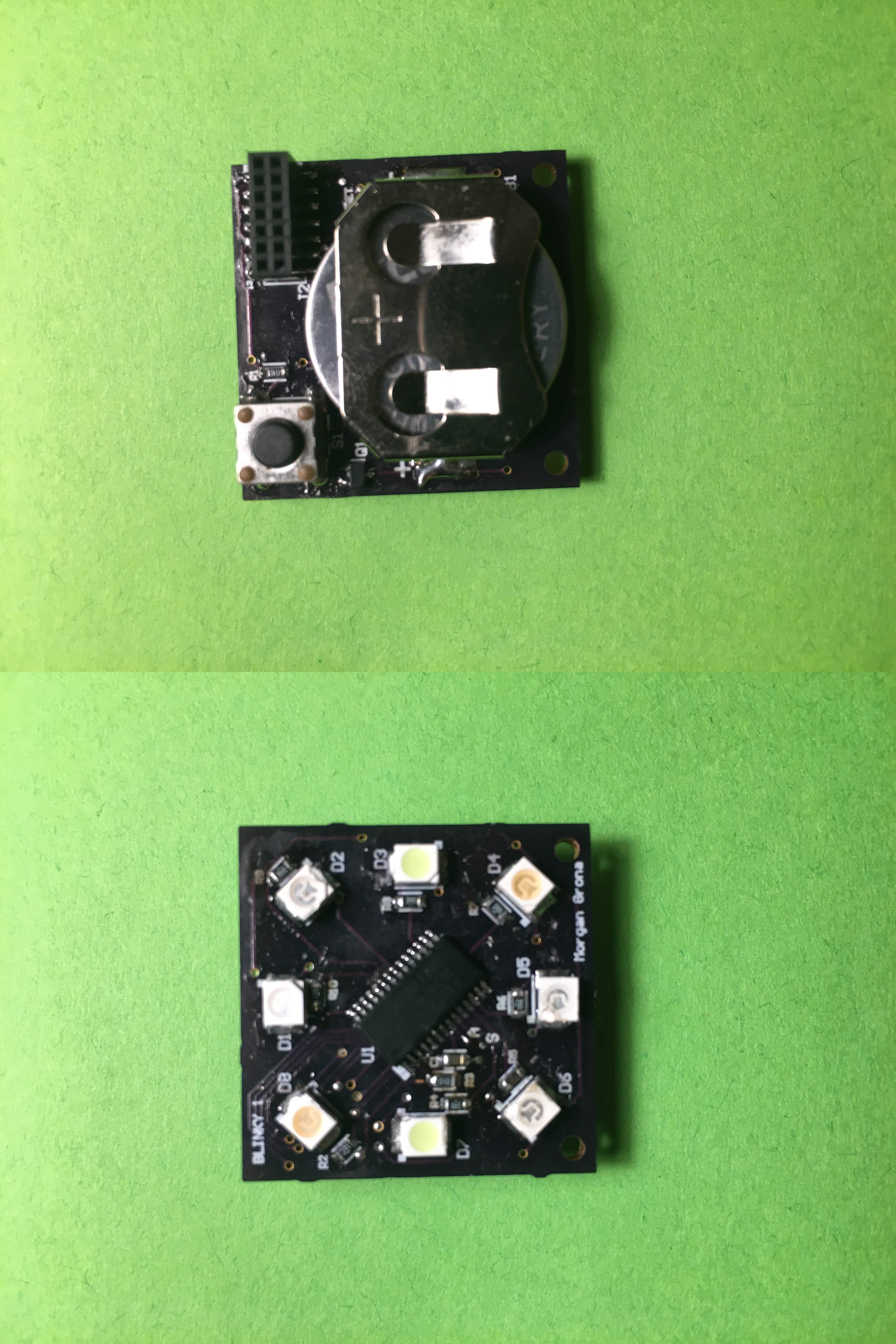 Populated PCB
Once the components are all mounted the device is ready to program.
This post is licensed under CC BY 4.0 by the author.